


Please Leave Us A Message
Privacy statement: Your privacy is very important to Us. Our company promises not to disclose your personal information to any external company with out your explicit permission.

Model No.: YZPST-T700123503BY
Brand: YZPST
Productivity: 100
Transportation: Ocean,Air
Place of Origin: China
Supply Ability: 1000
Certificate: ISO9001-2008,ROHS
HS Code: 85413000
Port: Shanghai
Payment Type: L/C,T/T,Paypal
Incoterm: FOB,CFR,CIF
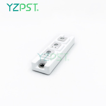
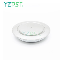
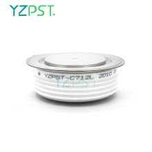
Phase Control Thyristors
YZPST-T700123503BY
Features of the Phase Control Thyristors: center amplifying gate configuration, compression bonded encapsulation, high DV/DT capability and stud type, thread inch or metric. The typical applications of the High Frequency Thyristors are medium power switching and DC power supplies.
Maximum Ratings And Characteristics
| Symbol | Parameter | Values | Units | Test Conditions | |
| ON-STATE |
|
|
| ||
| ITAV | Mean on-state current | 350 | A | Sinewave,180° conduction,Tc=85℃ | |
| ITRMS | RMS value of on-state current | 550 | A | Nominal value | |
| ITSM | Peak one cycle surge (non repetitive) current | 9.1 | KA | 10.0 msec (50Hz), sinusoidal wave- shape, 180o conduction, Tj = 125 oC | |
| I2t | I square t | 416 | KA2s | 8.3 msec and 10.0 msec | |
| IL | Latching current | - | mA | VD = 24 V; RL= 12 ohms | |
| IH | Holding current | - | mA | VD = 24 V; I = 2.5 A | |
| VTM | Peak on-state voltage | 1.4 | V | ITM = 625 A; Duty cycle £ 0.01%
| |
| di/dt | Critical rate of rise of on-state current | non-repetitive | 800 | A/ms | Gate drive 20V, 20Ω, tr≤1μs, Tj=Tjmax, anode voltage≤80% VDRM |
| repetitive | 150 | ||||
| BLOCKING |
|
|
| ||
| VDRM VRRM | Repetitive peak off state voltage Repetitive peak reverse voltage | 1200 | V |
| |
| VDSM VRSM | Non repetitive peak off state voltage Non repetitive peak reverse voltage | 1300 | V |
| |
| IDRM IRRM | Repetitive peak off state current Repetitive peak reverse current | 30 | mA | Tj = 125 oC ,VRRM VDRM applied | |
| dV/dt | Critical rate of voltage rise | 1000 | V/ms | TJ=TJmax, linear to 80% rated VDRM | |
| TRIGGEING |
|
|
| ||
| PG(AV) | Average gate power dissipation | 3 | W |
| |
| PGM | Peak gate power dissipation | 16 | W |
| |
| IGM | Peak gate current | - | A |
| |
| IGT | Gate trigger current | 150 | mA | TC = 25 oC | |
| VGT | Gate trigger voltage | 3.0 | V | TC = 25 oC | |
| VGD | Gate non-trigger voltage | 0.15 | V | Tj = 125 oC | |
| SWITCHING |
|
|
| ||
| tq | Turn-off time | 150 | ms | ITM=550A, TJ=TJmax, di/dt=40A/μs, VR=50V, dv/dt=20V/μs, Gate 0V 100Ω, tp=500μs | |
| td | Delay time | - |
| Gate current A, di/dt=40A/μs, Vd=0.67%VDRM, TJ=25 oC |
| Qrr | Reverse recovery charge | - |
|
|
Thermal And Mechanical
| Symbol | Parameter | Values | Units | Test Conditions |
| Tj | Operating temperature | -40~125 | oC |
|
| Tstg | Storage temperature | -40~150 | oC |
|
| R th (j-c) | Thermal resistance - junction to case | 0.1 | oC/W | DC operation ,Single sided cooled |
| R th (c-s) | Thermal resistance - case to sink | 0.05 | oC/W | Single sided cooled |
| P | Mounting force | 3.5 | Nm |
|
| W | Weight | - | g | about |

Product Categories : Semiconductor Stud Devices > Phase Control Stud Thyristor


Privacy statement: Your privacy is very important to Us. Our company promises not to disclose your personal information to any external company with out your explicit permission.
Fill in more information so that we can get in touch with you faster
Privacy statement: Your privacy is very important to Us. Our company promises not to disclose your personal information to any external company with out your explicit permission.