


Please Leave Us A Message
Privacy statement: Your privacy is very important to Us. Our company promises not to disclose your personal information to any external company with out your explicit permission.

Model No.: YZPST-STC2326
Brand: YZPST
Productivity: 1000
Transportation: Ocean,Air
Place of Origin: China
Supply Ability: 10000
Certificate: ISO9001-2008,ROHS
HS Code: 85413000
Port: SHANGHAI
Payment Type: L/C,T/T,Paypal
Incoterm: FOB,CFR,CIF
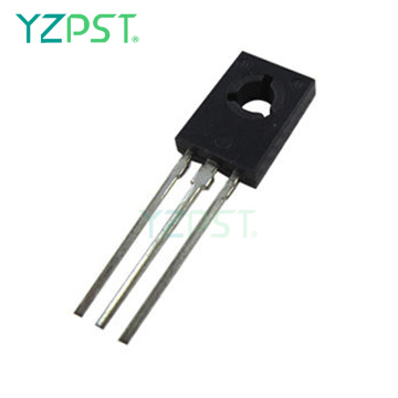
BTA30 Series Triacs
YZPST-STC2326
DESCRIPTION
The STC2326 is the N-Channel logic enhancement mode power field effect transistor which is produced using super high cell density DMOS trench technology. The STC2326 has been designed specifically to improve the overall efficiency of DC/ DC converters using either synchronous or conventional switching PWM controllers. It has been optimized for low gate charge, low RDS(ON) and fast switching speed.
APPLICATIONS
Powered System
DC/DC Converter
Load Switch
FEATURES
110V/3A,RDS(ON)=310mΩ@VGS=10V
High density cell design for extremely low RDS (ON)
Exceptional on-resistance and maximum DC current capability
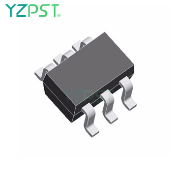
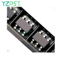
SOT-23-6L package design
PIN CONFIGURATION(SOT-23-6L)
")
| Pin | Symbol | Description |
| 1 | D | Drain |
| 2 | D | Drain |
| 3 | G | Gate |
| 4 | S | Source |
| 5 | D | Drain |
| 6 | D | Drain |
ORDERING INFORMATION
| Part Number | Package | Part Marking |
| SPN2326S26RGB | SOT-23-6L | 26YW |
ABSOULTE MAXIMUM RATINGS (TA=25℃ Unless otherwise noted)
| Parameter | Symbol | Typical | Unit | |
|
Drain-Source Voltage |
VDSS |
110 |
V | |
| Gate –Source Voltage |
VGSS |
±20 |
V | |
|
Continuous Drain Current(TJ=150℃) | TA=25℃ |
ID | 3.0 |
A |
| TA=70℃ | 2.0 | |||
|
Pulsed Drain Current |
IDM |
10 |
A | |
|
Power Dissipation | TA=25℃ |
PD | 2.0 |
W |
| TA=70℃ | 1.3 | |||
|
Operating Junction Temperature |
TJ |
-55/150 | ℃ | |
| Storage Temperature Range | TSTG | -55/150 | ℃ | |
| Thermal Resistance-Junction to Ambient | RθJA | 62.5 | ℃/W | |
|
Parameter |
Symbol |
Conditions |
Min. |
Typ |
Max. |
Unit |
| Static | ||||||
| Drain-Source Breakdown Voltage | V(BR)DSS | VGS=0V,ID=250uA | 110 |
|
|
V |
| Gate Threshold Voltage | VGS(th) | VDS=VGS,ID=250uA | 1 | 2.0 | 2.5 | |
| Gate Leakage Current | IGSS | VDS=0V,VGS=±20V |
|
| ±100 | nA |
|
Zero Gate Voltage Drain Current |
IDSS | VDS=80V,VGS=0V |
|
| 1 |
uA |
| VDS=80V,VGS=0V TJ=125℃ |
|
|
5 | |||
| On-State Drain Current | ID(on) | VDS≥5V,VGS =10V | 3.0 |
|
| A |
| Drain-Source On-Resistance | RDS(on) | VGS= 10V,ID=3A |
| 0.26 | 0.31 | Ω |
| Forward Transconductance | gfs | VDS=10V,ID=3A |
| 2.4 |
| S |
| Diode Forward Voltage | VSD | IS=1A,VGS =0V |
|
| 1.2 | V |
| Dynamic | ||||||
| Total Gate Charge | Qg |
VDS=80V,VGS=10V ID= 5A |
| 9 | 13 |
nC |
| Gate-Source Charge | Qgs |
| 2 |
| ||
| Gate-Drain Charge | Qgd |
| 1.4 |
| ||
| Input Capacitance | Ciss |
VDS=25,VGS=0V f=1MHz |
| 508 |
|
pF |
| Output Capacitance | Coss |
| 29 |
| ||
| Reverse Transfer Capacitance | Crss |
| 16.5 |
| ||
|
Turn-On Time | td(on) |
VDD=50V,RL=10Ω ID=3A,VGEN=10V RG=3.3Ω |
| 2 |
|
nS |
| tr |
| 21.5 |
| |||
|
Turn-Off Time | td(off) |
| 11.2 |
| ||
| tf |
| 18.8 |
| |||
")
")
Product Categories : Semiconductor Plastic Package > Silicon Transistor


Privacy statement: Your privacy is very important to Us. Our company promises not to disclose your personal information to any external company with out your explicit permission.
Fill in more information so that we can get in touch with you faster
Privacy statement: Your privacy is very important to Us. Our company promises not to disclose your personal information to any external company with out your explicit permission.